The 8-legged IC (Integrated Circuit) is the one of the most commonly used integrated circuits and this due to its ability to provide oscillations and time delays in a circuit when configured properly as we will see in the operation mode sector of the 555 timer, the 555 timer was first developed in the 1971 by Hans , the 555 timer gets it name from the three 5K ohms( 5 kiloohm) connected in series in the IC(integrated circuit) block diagram as I will discuss the internal blocks below.
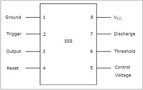
The 555 timers have gotten mainly three stages, and this is the voltage divider, the comparators and the flip-flop blocks. And all these are interconnected to process the input signal and make output at pin 3 in either and ON state or OFF state as we going to see below
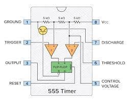
This block consists of three identical 5K Resistor connected in series dividing the input voltage from VCC (power pin) to GND (ground) and calculated so that the tap between the first and second Resistor outputs [2/3] of the input voltage (VCC) and the tap between the second and third outputs [1/3] of the input voltage (VCC).
This block has two comparators with the first comparator (positive terminal) connected to the threshold pin the negative connected to the voltage divider at the [2/3] tap and when the voltage of the threshold pin drops below [1/2] the output of the comparator goes to HIGH state and the output OUTPUT also goes to HIGH. And this continues as long as the TRIGGER voltage is kept LOW which is connected to the negative of the second comparator.
The output of the two comparators is connected to the inputs of the flip-flop R and S pins where the R input is connected to the output of the first comparator and the S connected to the output of the second comparator, the flip-flop operates in such a way that when the output of the first computer is HIGH and second one is LOW it outputs low which is then change at the output stage as HIGH which is connected also to the discharge transistor making the output pin HIGH and vise verses. The 555 timer also has an output stage that finally makes the output pin (pin 3) HIGH or LOW accordingly.
The 555 timer can be set in three common modes (configurations) depending on the circuits purpose these are the astable (free-running), monostable (one-shot) and bistable mode (latch) these being applicable in light flashers, touch switches and switch debouching respectively and all the configurations depends on the voltages applied to the Trigger, Threshold and Control Voltage Pins as we are going to see below
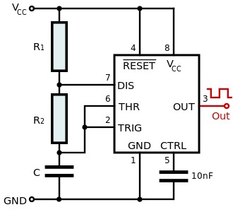
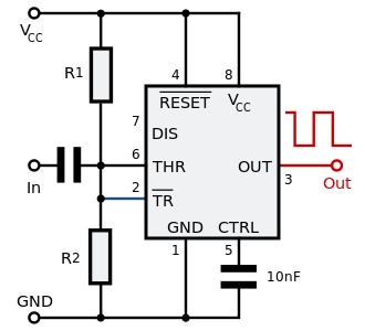
The Schematics of the Astable mode of the 555 timer is straight forward where the two resistor R1 and R2 are connected in series with a capacitor that is then ground this forms a voltage divider between R1 and R2 from which the discharge pin (pin 7) is connected giving the discharging path for the capacitor and the thresholds pins and trigger pins is shorted to keep both the pins HIGH and this cycle repeats whenever the capacitor voltage drops to [1/3] of the applied voltage. The Astable mode of the 555 timer finds use in PWM (pulse width modulation) and works as an oscillator circuit giving a continuous square wave at the output pin.
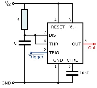
In the schematic diagram the resister R is connected in series with a capacitor C between the VCC and the GND, this CR circuit created provides the pulse duration (time) which is the time the capacitor takes to charge, in the monostable configuration of the 555 timer a pulse is produced at the output whenever the trigger voltage drops below [1/3] VCC in this mode the 555 timer finds use as a delay switch and a touch switch.
In this configuration the 555 timer threshold and trigger pins are both connected to the halved voltage gotten from the voltage divided by the two identical high resistors R1 and R2, the input signal is then feed through the a capacitor into the 555 timer with the control voltage capacitor at the pin 5 for the 555 timer which then trigger a clean pulse output at the output pin (pin 3) of the 555 timer.
Inconclusion the 555 timer is a widely used integrated circuit finding its use is most circuit board like the inverter circuits on television circuits, radio circuits etc. and it has help to accomplish a lot of electric projects so as an engineering student you have to really understand the works of the 555 timer because you will interface it a lot, so if you have learnt anything and still want to know about any other component and electric related projects let me know in the comments.